As I mentioned in my Sub-GHz Radio Modules project, I’m adding an SPI flash to store some information about the module, like the type and frequency band, to allow for auto-detection of the proper parameters. As such, I decided to pick up an old, unfinished project, of interfacing with SPI Flash. More specifically, SPI NOR Flash.
 SPI Flash speaks the same protocol across manufacturers, but there might be differences regarding which commands are implemented. The first steps I took when communicating with SPI Flash modules is reading the identification of the connected chip, using the REMS (0x90), RDID (0x9F) and RES (0xAB) commands. Please note, these names differ across the documentation by different manufacturers.
The RDID (0x9F) command returns three bytes, the manufacturer ID, the memory type and the memory density. The manufacturer ID is the ID provided by JEDEC in the JP106, which I have mentioned before when discussing JTAG. Please note, we only have one byte of manufacturer ID, we don’t know the bank ID. This means, we cannot tell manufacturers apart which share the same manufacturer ID on a different bank.
The memory type field as well as the memory density field are manufacturer specific. All though it seems there exist a convention that says the capacity of the chip is 2memory_density, for chips up to and including 256 mebibit (32 mebibyte). There is a discontinuity for larger chips. See the flash implementation in esp-idf. However, looking at what distributors sell, these larger chips are rare for NOR Flash. It seems this is the size when NAND Flash becomes in use. Be aware the size of flash chips is measured in bits rather then bytes. Also, I am using the mebi prefix in stead of mega to differentiate 1024 vs 1000.
Some flash chips might also implement the SFDP command. Using the SFDP command, one can retrieve data structures that describe the capabilities of the chip. This includes the size, and the supported read/write modes (for example, 2 or 4 wire modes, aka QSPI), and what erase commands are supported.
SPI NOR Flash is organised in pages (256 byte), sectors (4 kiB) and blocks (32 or 64 kiB). Some flash chips support erasing pages, but most commonly, a sector is the smallest erasable size. Be aware one cannot overwrite flash content. A write can only flip a 1 to a 0. So, you can turn 0b10101010 to 0b10000010 by writing to the same address, but when you want to turn a 0 into a 1, one must erase. This is why the minimal erasable size matters. Being able to erase smaller chunks of memory deduces the number of erase/write cycles, thus reducing flash wear.
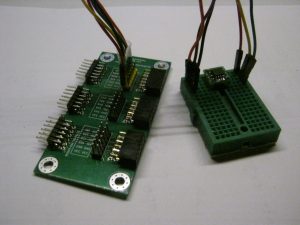
I have various SPI NOR Flash around from different brands. GigaDevice, Puya, Winbond, XMC. While reading and writing to the GigaDevice, Puya and Winbond chip works fine, I ran into some issues when communicating with the XMC chip.
Basic commands, rdid, rems and res appear to work as advertised
REMS 20
RDID 20 40 16
RES  15
However, trying to read the SFDP gives unexpected data:
 Expected: 53 46 44 50
 Received: A6 8C 88 A0
It looks like the data has been shifted one bit to the left. Also reading its memory content seems to be affected the same way:
Read back:
01 FF FF FF  FE 84 D8 C2  C2 E9 FF FF  FF FF FE C2     ................
C4 C6 C8 CA  CC CE D0 D2  D4 D6 D8 DA  DC DE E0 E2     ................
E4 E6 E8 EA  EC EE F0 F2  F4 C2 C4 C6  C8 CA CD FF     ................

Expected:

00 FF FF FF  FF 42 6C 61  61 74 FF FF  FF FF FF 61     .....Blaat.....a
62 63 64 65  66 67 68 69  6A 6B 6C 6D  6E 6F 70 71     bcdefghijklmnopq
72 73 74 75  76 77 78 79  7A 61 62 63  64 65 66 FF     rstuvwxyzabcdef.
I decided to connect my logic analyser to see what was going on. And looking at the logic analyser, 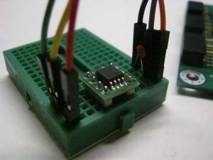 I didn’t see anything wrong. Looking at the output of my code, it also seemed to work. When I removed the logic analyser, the problem returned. This made me think, adding those logic analyser wires adds capacity to the bus. So, I tried putting a small capacitor between MOSI and GND. Intuitively, putting capacitors between MOSI and GND line feels wrong, but it seems this fixed the issue. My theory, these Dupont wires and breadboard aren’t great, and add some clock skew. As the microcontroller control the CLK line, and the flash chip controls the MOSI line, this clock skew causes the signals at the microcontroller to get out of sync. Adding some capacitive load directly at the flash chip brings it back in sync. I guess I should have a look with a scope rather then a logic analyser.
I have had trouble using a DS1302 RTC chip on the end of a ribbon cable. On the transitions of the clock signal ringing would send the signal below the ground level and the DS1302 would not respond correctly. I added 100 ohm series resistors and 10pF or 100pF capacitors to ground at the DS1302. I am curious about what you would see with a scope at the clock input to the flash chip.
My apologies I only see this now.