 One of my goals these holidays were to design some new ucdev baseboards. I’m looking at the ESP32C3 and ESP32S3. Now, there are various boards on AliEbay, so which one to design for. When I bought some samples last March. Back then I went for the NodeMCU models. However, looking at AliEbay today, it seems another variant has gained popularity, a variant by vcc-gnd.com.
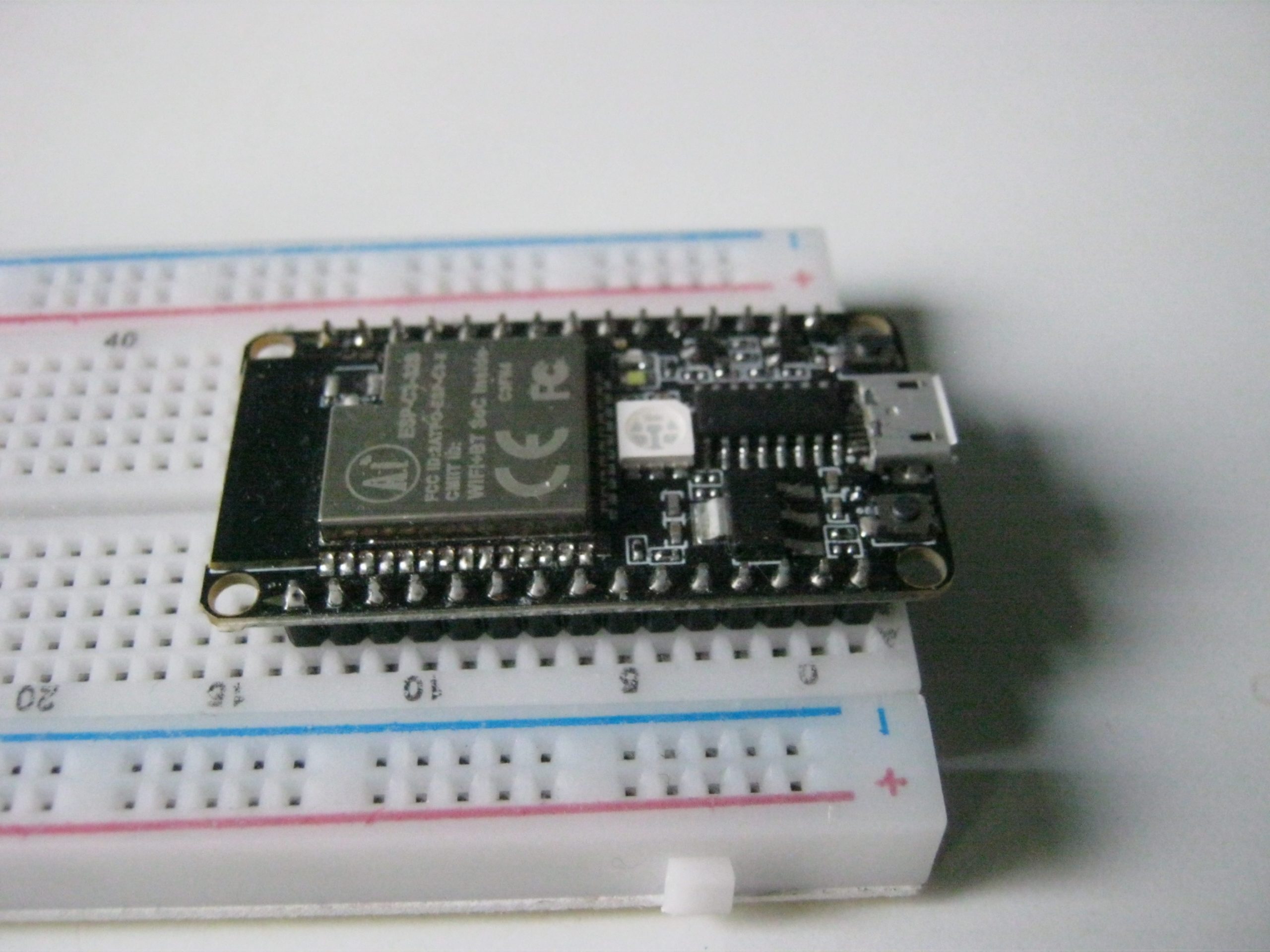
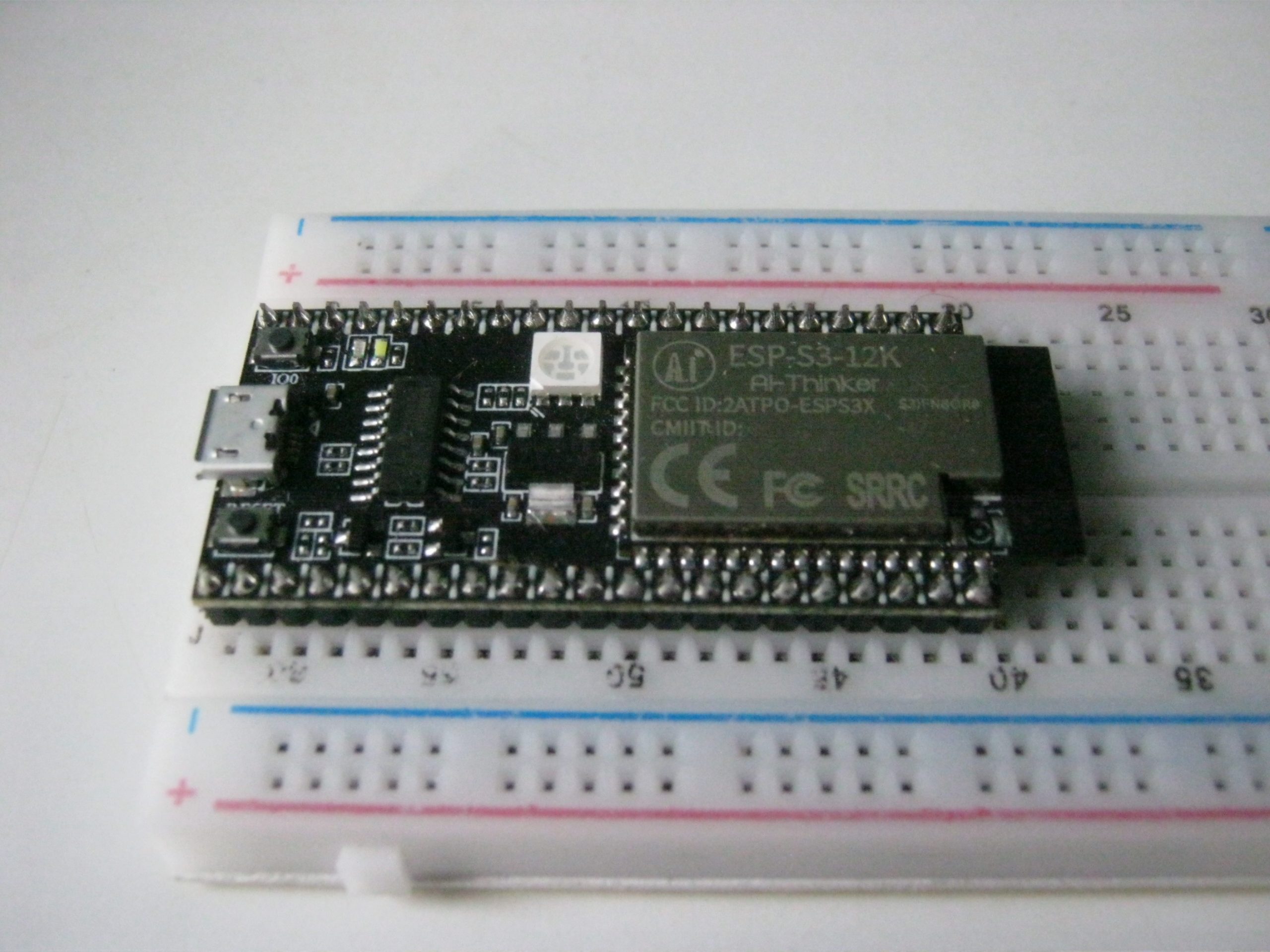 These NodeMCU boards are nice for actually fitting into a breadboard. But they have no pin labels at top, so when you put them in a breadboard, you’ll have to look up the documentation, which shows the bottom view, so you’ll have to mentally swap them. But at least it fits into a breadboard.
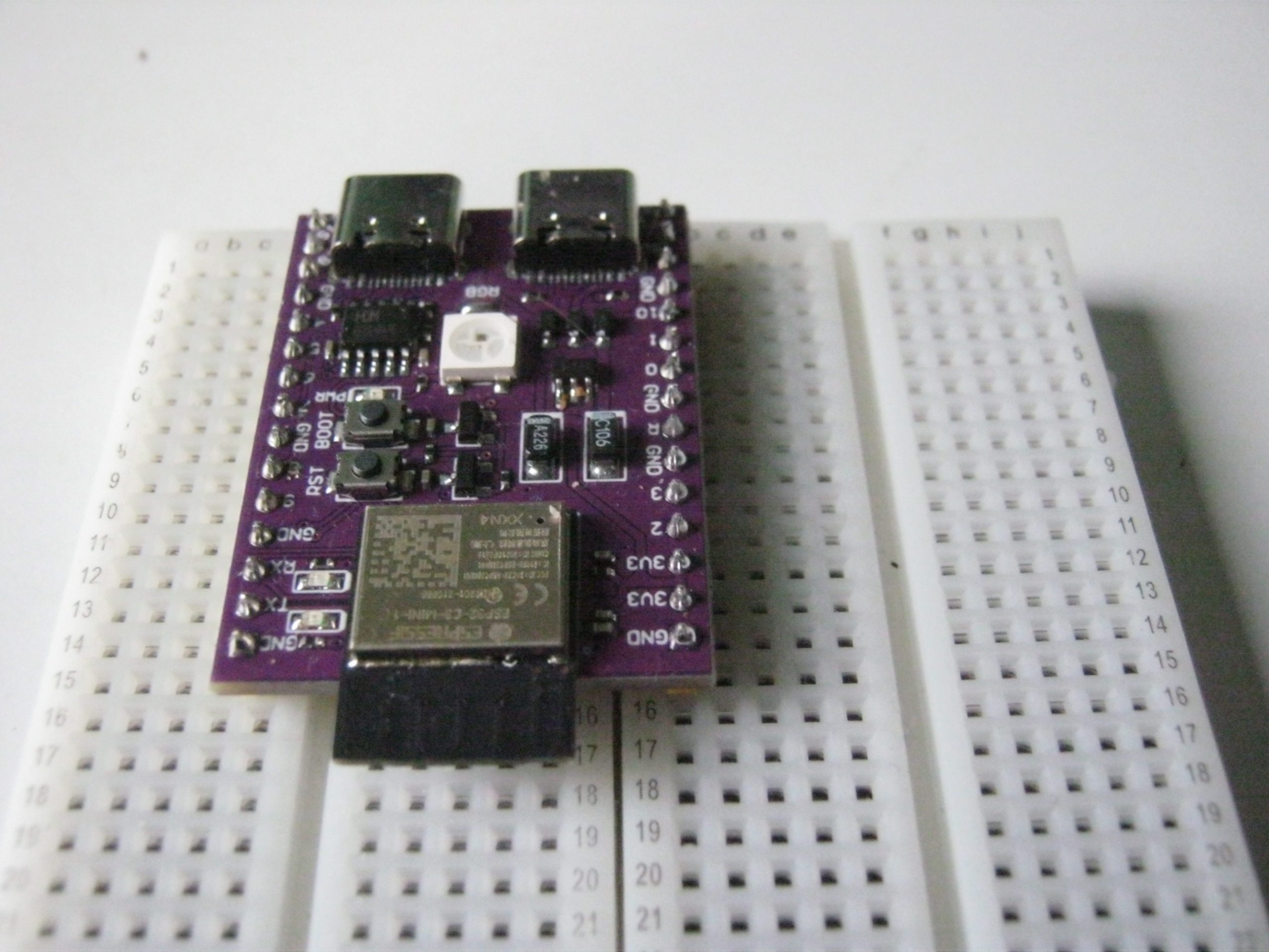 The vcc-gnd boards are annoying when attempting to use them in a breadboard. It would require taking two breadboards, removing their power rails, and snapping them together, in order for these boards to fit. However, these boards have their pins labelled, so it’s more convenient to hook up. Another thing to note is that these boards have two USB ports, rather then one as on the NodeMCU boards.
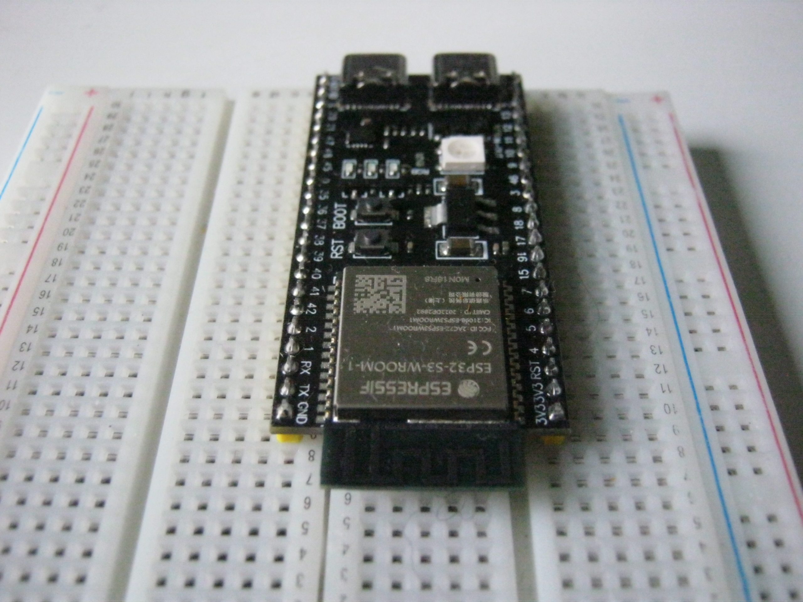 The NodeMCU boards use regular micro usb ports, while the vcc-gnd boards use USB type C ports. While as usual on ESP32 boards, the USB port is connected to an UART bridge, which allows for flashing using a bootloader in ROM. For the models with two USB ports, the second port is hooked up to the ESP32{C/S}3 directly. The ESP32{C/S}3 provides native USB support, which exposes a debugger “JTAG” interface.
As it seems, when searching AliEbay, the vcc-gnd design is the most common. As I am designing by own baseboard, the width of the board doesn’t matter. I’ll so with the vcc-gnd board. The ESP32S3 has plenty of GPIO pins, which can be used for any digital function. This allows for fully populating the PMOD connectors, and have a header for an external JTAG debugger (next to the internal one). The ESP32C3 on the other hand, has a low number of GPIO pins. On that board, they have many pins connected to GND, so it looks bigger then it is.
Furthermore, I’m looking at the HK-W801 and HK-W806 boards. These boards… they have a totally different pinout, despite being based on basically the same chip, with as main difference the antenna pin to be N/C on the W806. When looking into these boards, I’ve discovered an annoying aspect in these chips. The W80x has two options for the pins for I²C, They are either on UART0, which is connected to an USB-UART bridge, used for programming the chip. As these are hard-wired on the boards, this ain’t an option. The other option are the pins that are also used for the debugging interface (CKLink Lite). So basically, this is the only option, and disabled debugging support. This is a rather annoying configuration. I’m designing a boards, where I can jumper these pins to either the PMOD connector or the debugger header. Not ideal, but that’s the best given the options.